

Nanostructure resonators for enhanced absorption in thermoelectric photodetectors
Technology title
Nanostructure resonators for enhanced absorption in thermoelectric photodetectors
Technology overview
The invention relates to cascaded resonant nanoscale thermoelectric photodetectors that utilise both n-type and p-type thermoelectric materials. Unlike conventional semiconductor-based photodetectors, this technology is not limited by bandgap constraints and is capable of broadband light detection. By incorporating resonant nanostructures made from bismuth telluride (Bi₂Te₃) and antimony telluride (Sb₂Te₃), the device enhances optical absorption and improves photosensitivity. The cascaded configuration enables efficient conversion of absorbed light into electrical signals via the photo-thermoelectric effect, making it suitable for applications in sensing, optoelectronic communications, and wide-temperature-range detection.
Technology specifications
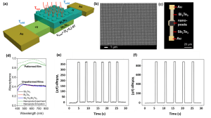
The technology comprises a cascaded thermoelectric photodetector integrating nanoscale resonant structures formed from n-type Bi₂Te₃ and p-type Sb₂Te₃ materials. The nanostructures are patterned using lithographic techniques and deposited onto a substrate to enable localised optical absorption and thermal gradient generation.
Upon illumination, the resonant nanostructures induce localised heating, creating a temperature gradient across the thermoelectric materials and generating a voltage via the Seebeck effect. The cascaded device structure enables efficient signal generation and collection. The device also supports bidirectional light absorption through its structural design, contributing to improved photodetection performance.
Sector
The invention is applicable to the photonics and optoelectronics sector, particularly in sensing, optical communications, and broadband photodetection applications.
Market opportunity
Plasmonic thermoelectric photodetectors represent an emerging alternative to conventional commercial photodetectors, which currently dominate a mature USD 20–30B global market driven by high-performance, low-cost CMOS and photodiode technologies. Rather than competing directly on sensitivity or speed, this technology targets niche, high-value applications where conventional devices are less suitable, offering unique advantages such as self-powered operation (no external bias), nanoscale spectral tunability, and multifunctional integration of optical, thermal, and electrical responses in a single material platform. These features position it strongly for integrated photonics, miniaturised spectrometers, and next-generation IoT or harsh-environment sensing, where system-level simplification and functionality outweigh absolute performance.
Applications
Key applications include optical sensing and detection, optoelectronic communications, broadband photodetection, and scientific instrumentation.
Customer benefits
Customer benefits include improved photosensitivity and detection accuracy, enabling more reliable performance even under low-light conditions. The bidirectional light detection capability offers greater design flexibility, allowing easier integration into a wide range of device architectures. In addition, the technology provides enhanced efficiency and stability of signal generation, while reducing the need for additional processing steps, making it suitable for scalable and practical applications.
Technology readiness level
TRL 3-4
Ideal collaboration partner
Some ideal collaboration partners include semiconductor and photonics companies, sensor and imaging system manufacturers, and advanced materials or nanofabrication foundries with capabilities in thin-film deposition and nanoscale patterning. Industrial partners with experience in device processing, wafer-scale fabrication, and device packaging would be particularly valuable to accelerate translation. In addition, collaborations with system integrators (e.g., IoT, visible sensing, or spectroscopy platforms) are desirable to validate application-specific performance.
Collaboration opportunities are open to any companies interested in developing grayscale photodetectors or imaging sensors with greater radiation robustness than traditional CMOS.
Collaboration mode
This technology is suitable for multiple collaboration modes, including joint research and development (R&D) to optimise device performance and architecture, technology licensing for integration into existing photodetector or sensing platforms, and co-development agreements with industry partners targeting specific applications (e.g., integrated photonics or self-powered sensors). Opportunities also exist for prototype development and pilot-scale fabrication, as well as industry-sponsored research projects to advance scalability, reliability, and system-level integration. Depending on partner interest, pathways may extend to commercialisation partnerships or spin-off formation.
- R&D collaboration: Optimise device design, materials, and scalable fabrication.
- Licensing: Enable integration into photonic and sensing platforms.
- IP acquisition: Strengthen portfolios in plasmonics and thermoelectric photodetection.
- Test-bedding: Collaborate with industry for real-world validation, reliability assessment, and application-specific optimisation (e.g., IoT sensors, integrated photonics, miniaturised spectrometers).