
Singapore University of Technology and Design (SUTD)
Master of Science in Technology and Design (Integrated Photonics For Semiconductor Technology)
Programme schedule
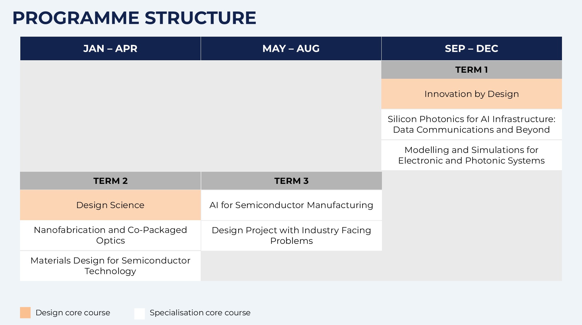
The MTD (Integrated Photonics for Semiconductor Technology) is a one-year full-time coursework-based Master programme. It comprises eight courses (96 credits): two core design courses and six specialised courses, organised as follows:
Course descriptions
Innovation by Design (12 credit points)
The focus of this course is the integration of marketing, design, engineering and manufacturing functions in creating and developing a new product, system or service. The course will go through the different phases of designing a new product, system or service using the four Ds of the four-phase Design Innovation Cycle of “Discover-Define-Develop-Deliver”. The course will focus on some of the critical success factors for new product development, with an early emphasis on design thinking. Students will be given a design challenge to complete.
Silicon Photonics for AI Infrastructure: Data Communications and Beyond (12 credit points)
Silicon Photonics for AI Infrastructure: Data Communications and Beyond provides a practical introduction to photonic integrated circuits for high-speed optical interconnects, AI data centres, and emerging applications. The course covers the full workflow from device principles and circuit design to GDS layout, foundry tapeout, packaging, testing, and performance analysis. Students will gain hands-on experience through industry-oriented design and measurement exercises.
Modelling and Simulations for Electronic and Photonic Systems (12 credit points)
As devices become increasingly complex and are engineered at ever-smaller scales, computational modelling and simulation is indispensable for predicting device behavior, optimising performance, and reducing costly fabrication iterations. This course equips students with the knowledge and practical skills to model, analyse, and optimise electronic and photonic systems using numerical methods and industry-relevant simulation tools. Through laboratory exercises and project-based learning, students will gain hands-on experience with Python and MATLAB for numerical modeling, TCAD tools for semiconductor device simulation, SPICE-based circuit simulators for electronic circuit analysis, and Ansys Lumerical FDTD simulation for the design and analysis of integrated photonic devices. The course also introduces emerging AI-driven techniques, such as machine learning algorithms and inverse design, to accelerate the development of next-generation semiconductor technologies.
Design Science (12 credit points)
This course introduces students to design science where many design principles and methods will be reviewed, applied and analysed. Students will learn to make connections between design science and other fields, such as engineering, and how principles in design science can be used to advance these fields. The class will cover a broad set of design methods such as customer needs analysis, methods in creativity, functional modelling, design for X and design for testing and verification.
Nanofabrication and Co-Packaged Optics (12 credit points)
The rapid growth of AI, cloud computing, and hyperscale data centres is driving the adoption of Co-Packaged Optics (CPO), where photonic devices are integrated alongside electronic processors to deliver unprecedented bandwidth and energy efficiency. This course introduces the nanofabrication technologies that enable modern photonic integrated circuits and CPO systems. Students will learn the complete device fabrication workflow, including thin-film deposition, optical and electron-beam lithography, nanoimprint lithography, etching, and nanometrology. A distinctive feature of the course is hands-on training in the SUTD Cleanroom and Nanometrology Laboratories, where students will fabricate and characterise photonic device components using state-of-the-art semiconductor processing and characterisation equipment. The practical skills developed in this course provide a strong foundation for designing and manufacturing next-generation photonic hardware for AI, high-performance computing, optical communications, and data-centre applications.
Materials Design for Semiconductor Technology (12 credit points)
This course covers the use of different TCAD device modelling and simulation software tools to guide in the choice of materials for logic and memory devices and assess the electrical–mechanical–thermal co-design of devices, circuits, and packages through the use of multiphysics simulation tools.
AI for Semiconductor Manufacturing (12 credit points)
The complexity and data-driven demands of the fields that optics and photonics engineering is playing in increasingly require advanced AI methods. This course bridges the knowledge gap between optical science and AI, equipping students with practical skills in applying machine learning to photonic device design, optical communications, imaging, and large-scale data analysis. Students will learn to deploy AI-driven optimisation, integrate AI with traditional physics-based modeling, and evaluate the effectiveness and limitations of AI approaches in photonics, preparing them for competitive roles in research and industry.
Design Project with Industry Facing Problems (12 credit points)
Mentored by an SUTD faculty member, students in groups will work on a semester-long optics and photonics design project partnered with industry.