Academic facilities
About us
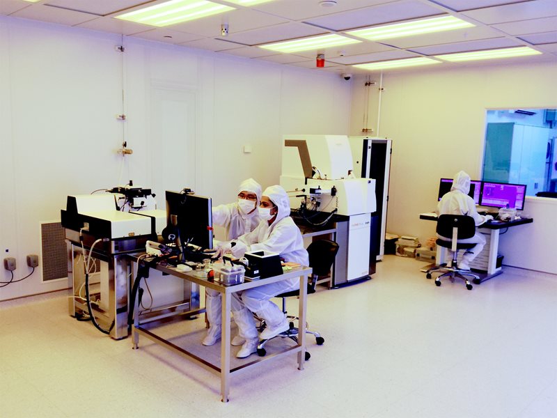
Established in August 2015, the SUTD Cleanroom is designed to facilitate the complete semiconductor process, nanofabrication, and precision machining for undergraduate and graduate students, and research fellows. The Class 1000 Cleanroom provides a safe work environment and features a fully automated building management system (BMS) and innovative state-of-the-art facilities.
The Cleanroom equipped for various nano-engineering processes, such as electron beam evaporation, electron beam lithography, reactive ion etching, nano-imprinting lithography, nano scribe, thin film depositions, ellipsometry, profilers, microscopes, and different unique lithography techniques.
Facilities
The SUTD Cleanroom is committed to serve faculty, researchers, students, industry professionals, and the broader scientific community. We offer services such as workshops, collaborative research projects, and opportunities for knowledge-sharing.
We focus on creating a community of practice at SUTD and promoting collaboration with other universities and institutions to ensure everyone is valued and included in our mission.
Our ISO Class 6 / Class 100 Cleanroom is equipped with the following facilities:
- Fully automated cleanroom management system
- Extensive gas leak detection system
- Intensive fan filter management system
- Cleanroom equipment booking system
- Kanban consumable management techniques
- Smart gowning techniques
- Automated scheduled cleanroom hygiene
- Telescope robotic assistance
- SMED (Single-Minute Exchange of Dies) implementation for critical facilities
Get in touch with us if you are interested in contributing or collaborating with us.
Equipment and services
- Electron beam lithography
Raith e-line plus – offers high-resolution patterning capabilities, enabling the creation of features as small as sub-10 nm. - 3D laser writing
Photonic Professional GT (Nanoscribe) – creates nano-, micro-, and meso-structures with feature sizes starting from about one hundred nanometres and achieving layer thicknesses well below 1 µm. - Electron beam evaporation
Kurt J Lesker – is used for the physical vapour deposition of materials such as gold, titanium, silver, chromium, platinum, silicon dioxide, and aluminium. - Nano-imprint lithography (NIL)
Model NX-2000 (Nanonex) – achieves sub-5 nm resolution and 1% CD control, producing high-throughput, sub-10 nm structures at low cost. - Mask alignment
EVG610 – handles small substrate pieces and wafers up to 200 mm, supporting various lithography processes and specialized applications. - Sputtering deposition
ATS500 HHV and CUBE Balzer – deposits thin films of materials like Ti, Al, Ag, Sb2Te3, TiW, SiO2, and TiO2 through ion bombardment in a controlled vacuum environment. - Rapid thermal processing (RTP)
ECOPIA RTP-1300 – heats semiconductor wafers to temperatures up to 1300°C, enabling precise thermal treatments for applications such as dopant activation and annealing. - Contact profilometry
KLA-Tencor D600 – measures step height and surface roughness in thin films using a stylus. It offers high vertical resolution, typically in the range of 1 nm. - Non-Contact Optical 3D Profilometry
KLA Profilm 3D – uses optical techniques to measure surface topography, film thickness, roughness, and texture without physical contact. It offers high vertical resolution, typically in the range of 0.5 nm. - Spectroscopic ellipsometry
Accurion EP4 – provides precise measurements of film thickness (from 0.1 nm to several microns), refractive index, and optical constants for thin, transparent, or multi-layer films.
Contact us
We welcome collaborations with the SUTD research community, industry professionals, and the broader scientific community. If you are interested in contributing, please get in touch with us.
Cleanroom @ SUTD
8 Somapah Road
Building 2, Level 2 (Room 2.207)
Singapore 487372
Telephone: 6876 4267
If you are driving to SUTD, please use the Cleanroom entrance at Building 2 Lobby F.
Our faculty
YANG Joel
Professor
Associate Head of Pillar (EPD) (Research and Advancement)
Director (Cleanroom)
AI Ye
Associate Professor
Co-Deputy Director (CHEERS)
DONG Zhaogang
Associate Professor
TAN Dawn
Associate Professor
Provost’s Chair Professor